

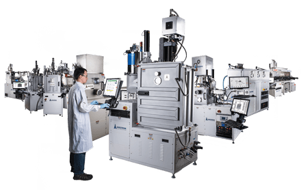

OLED Development using the Nebula Cluster
Thanks to developments in organics, the thin-film display industry is making remarkable leaps forward. Organic materials have proven themselves as viable, and in many cases, the preferred components for these displays by manufacturers, investors, and consumers. For those looking to innovate within the industry, ease and speed of development are required for any sort of competitive advantage. Angstrom Engineering's Nebula Cluster is the ideal tool for OLED material development and device fabrication, as it combines ease of use, fully automated device processing, and unequivocal partner support, providing the industry's best possible path to market.
Demonstrable OLED Success in 3 Steps
1. Proven Process Stability
Angstrom Engineering has worked in the OLED industry for decades, providing tools to many of the pioneers of the technologies, and has helped them scale it to where it is today.1 We have built Nebula Cluster systems as OLED-specific development tools, and our partners are achieving impressive milestones with them.
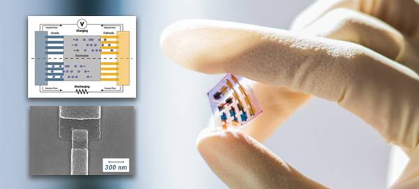
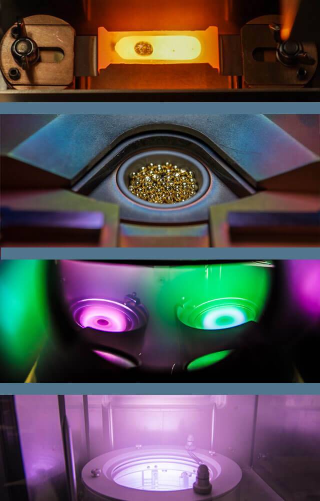
The core of any OLED development tool is the physical deposition of materials utilizing thermal evaporation, sputtering, electron-beam evaporation, ion beam processing, and plasma processing. Hundreds of Angstrom Engineering machines are currently being employed across the globe utilizing these technologies, and the user feedback suggests that these tools make up the heart of their fabrication facilities.
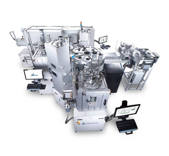
2. Unprecedented Automation
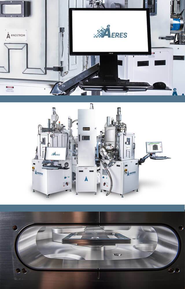
Thin Film processing has changed drastically over the past 5 years, and Angstrom Engineering has been at the forefront in helping bring about that change. An in-house software development team has created Aeres®, a disruptive collection of code that integrates every aspect of fabricating OLED devices. This advanced process control software makes it possible to enter every variable of device fabrication through its intuitive recipe builder, press 'go', and walk away confident that even the most complex pixel architectures will be made into matter without direct user inputs. Repeatability is the focus, so that you can finesse your devices knowing that extraneous variables will be far from your mind.
While novice users can create repeatable films with minimal training, the intuitive user-interface allows expert users to dive into every variable in detail.
Rapid OLED development requires multiple processing steps, as well as the ability to create multiple devices simultaneously, necessitating independent deposition modules for substrate preparation, metals and organics deposition, along with the means to automatically transfer samples between them all. Aeres®, along with the employment of state of the art robotics, handles everything in situ, allowing the creation of hundreds of architectures over 20 plates to be fabricated in a single day. Press go, and come back to hundreds of complete OLED devices.
3. Human Support
Every individual at Angstrom Engineering orbits around an ethos of doing everything we can to help our partner's work move forward. The most common feedback we receive from our partners is surely the most important: we support them and their work in real, tangible ways, and make it easier for them to succeed. The purchase and installation of a Nebula Cluster for rapid OLED development is the beginning of a relationship to which we are committed.
Let us prove it to you. Get in touch regarding your OLED work and let's discuss together how Angstrom can help you compete, and stay out in front, in this exciting field.
Let's talk OLED.
Please get in touch and we can collaborate on your OLED development work.