ETH Zurich Advances OLED Pixel Manufacturing with Photolithography
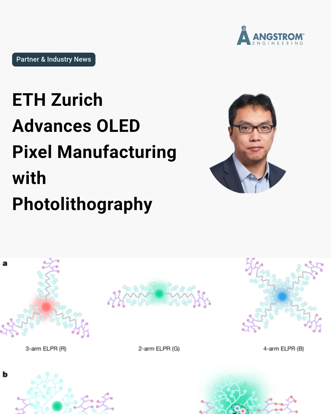
Researchers at ETH Zurich have developed light-emitting polymers that can be patterned using photolithography, an established process used in semiconductor manufacturing. The new materials can withstand the chemical conditions involved in the process, allowing extremely small, coloured OLED pixels to be created with high precision.
The team demonstrated the approach by producing a multicolour fluorescent image measuring just 300 by 430 micrometres and consisting of 250 by 350 pixels. The method could support smaller, sharper displays, along with precise light sources for applications in microscopy, sensors, and biological and medical research.
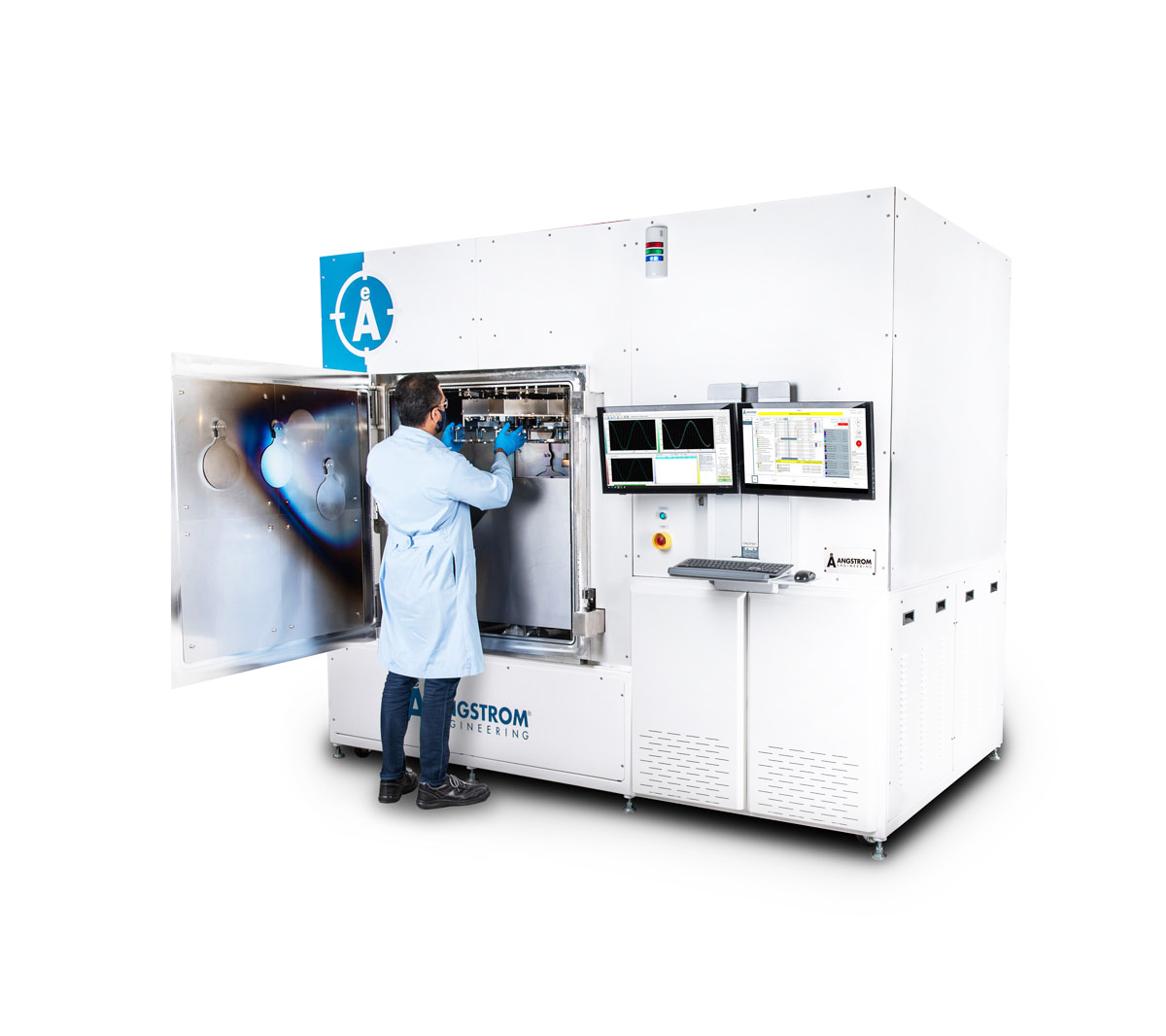
Prof. Chih-Jen Shih’s group at ETH Zurich uses five customized Angstrom Engineering PVD systems integrated with gloveboxes to support their research. “These systems have been very robust and reliable, with user-friendly and precise automation, which significantly accelerated the process development and optimization,” says Shih. “We can always reproduce the results even dealing with the demanding top-emitting devices.”