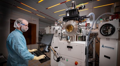
by Andrew Goodwin | Apr 14, 2026 | Angstrom Engineering News
April 14 marks World Quantum Day, a celebration of the science and technologies shaping the next era of computing, communication, and discovery. The date itself reflects Planck’s constant (4.14 × 10⁻¹⁵ eV·s), a fundamental value at the core of quantum mechanics and a...
by Andrew Goodwin | Feb 12, 2026 | Partner & Industry News
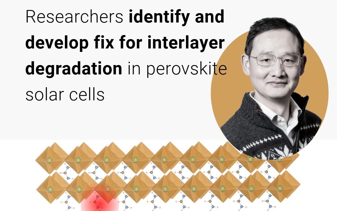
Dr. Chingbin Fei, Dr. Jinsong Huang, and a team of collaborators from the University of North Carolina at Chapel Hill (and University of Colorado-Boulder) have identified how device interlayers were ‘poisoning’ perovskite solar cells over time, and...
by Andrew Goodwin | Jan 20, 2026 | Partner & Industry News
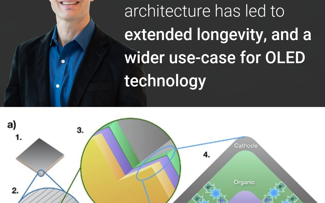
Our partners in the Giebink Lab at University of Michigan, along with collaborators, have created a novel, high aspect-ratio OLED device architecture that uses “microscale ridges to pack more OLED into a given lighting panel area and lasts 2.7 times as long,...
by Andrew Goodwin | Jan 8, 2026 | Partner & Industry News
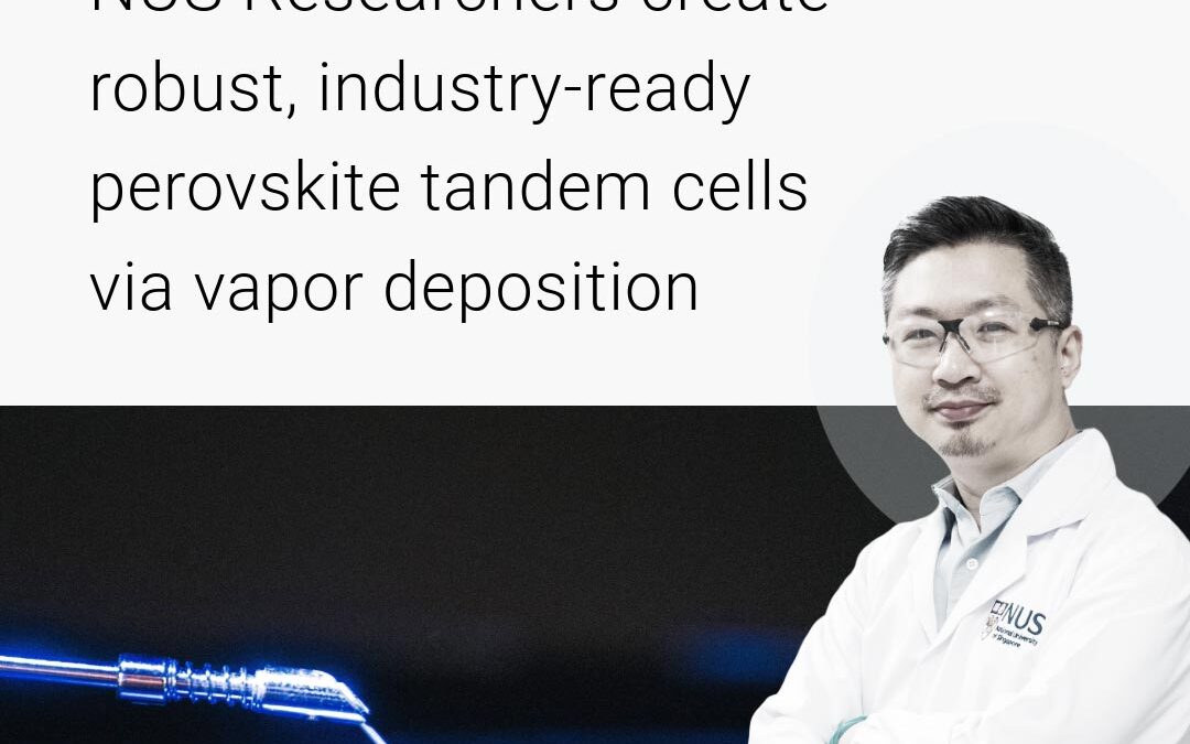
Longstanding engineering challenges have been the focus of thin-film perovskite optoelectronic devices since their discovery as a contender for the ‘next best’ photovoltaic material. Dr. Hou’s team have now demonstrated that utilizing vapor...
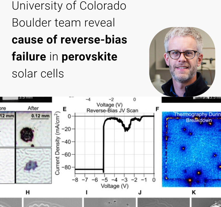
by Andrew Goodwin | Nov 20, 2025 | Partner & Industry News
Dr. Mike McGehee and colleagues at the University of Colorado Boulder, in collaboration with NREL, have uncovered why perovskite solar cells “melt” under stress. Their research revealed that microscopic defects such as pinholes and thin spots in the perovskite layer...