by Andrew Goodwin | Oct 7, 2025 | Partner & Industry News
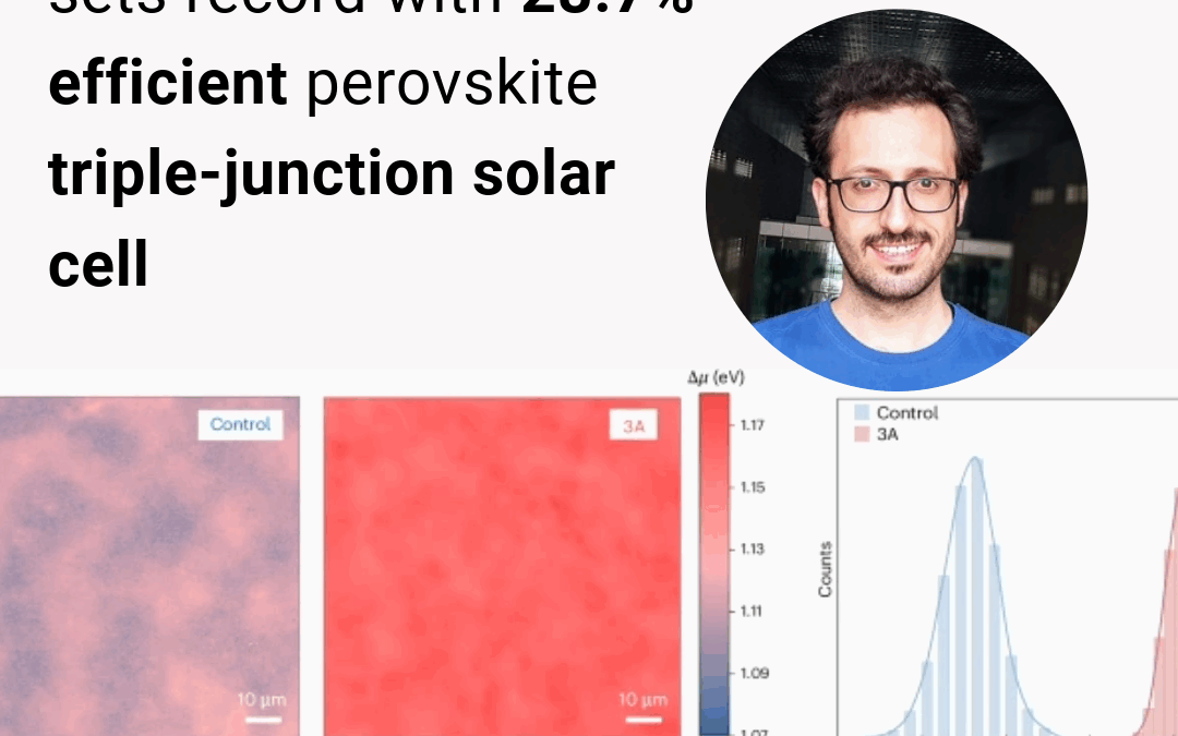
Partners at King Abdullah University of Science and Technology (KAUST), in collaboration with international partners, have achieved a new record: a 28.7% efficiency perovskite–perovskite–silicon triple-junction tandem solar cell. This device uses stabilized perovskite...
by Andrew Goodwin | Sep 18, 2025 | Partner & Industry News
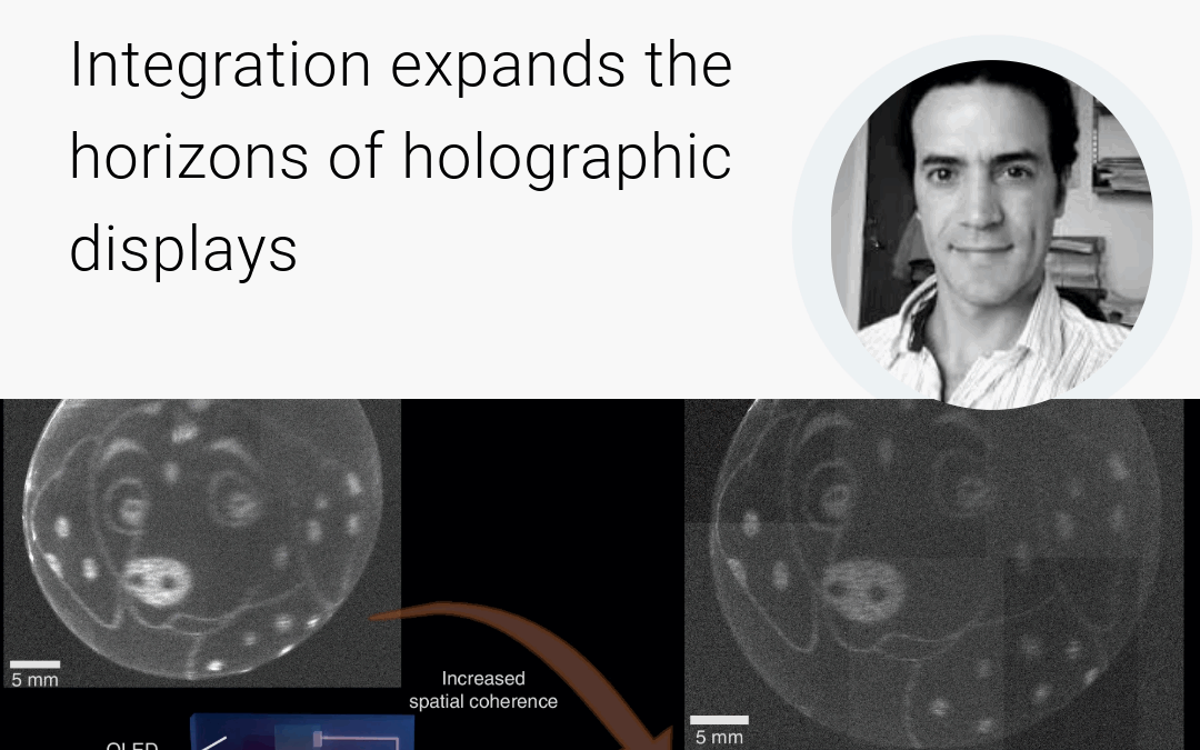
Dr. Andrea Di Falco and colleagues at the University of St Andrews have achieved a breakthrough in holographic technology. They combined organic light-emitting diodes (OLEDs) with holographic metasurfaces (HMs), delicate arrays of nanostructures that manipulate light....
by Andrew Goodwin | Sep 3, 2025 | Partner & Industry News, Perovskite
IMEC researchers, in collaboration with Hasselt University, EnergyVille, KU Leuven, the Aerospace Lab, and the University of Oklahoma, have demonstrated the strong potential of perovskite solar modules for future space applications. These conditions include...

by Andrew Goodwin | Jul 23, 2025 | Partner & Industry News
Dr. Yi Hou and his group have made progress in tandem perovskite cells. The National University of Singapore researchers utilized the unique bandgap-tunable properties of both perovskite and the stacked organic layers to gain the benefits of perovskite while not being...
by Andrew Goodwin | Jul 7, 2025 | Partner & Industry News
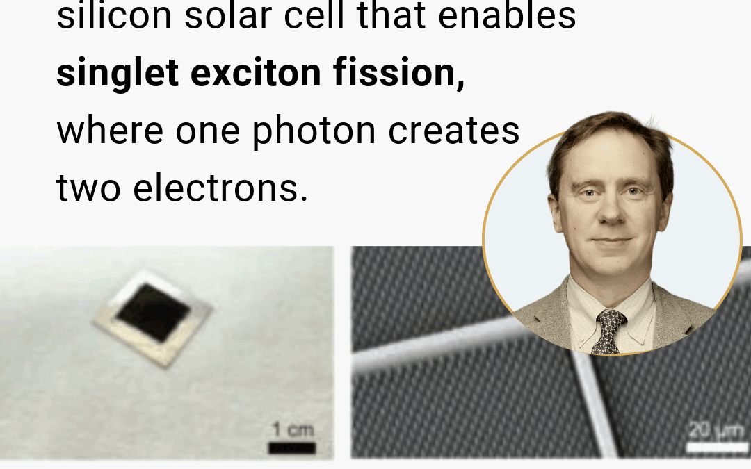
Our partners in the Baldo group at MIT have published their recent work in silicon solar cells that demonstrate the possibility of singlet exciton fission. “Key to their achievement was an interface that transfers the electrons and holes sequentially into...