How Do You Solve A Problem Like Perovskite?

As part of our year-end review of all the amazing research our partners are doing with our equipment (which you can find here), we’re sharing what 6 of our partners are doing to solve the challenges that perovskite materials present.

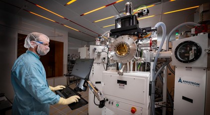
KAUST (King Abdullah University of Science and Technology) houses many Angstrom Engineering thin film evaporation and sputter systems in various labs, and is a hotbed for Perovskite research.

KAUST (King Abdullah University of Science and Technology) houses many Angstrom Engineering thin film evaporation and sputter systems in various labs, and is a hotbed for Perovskite research.

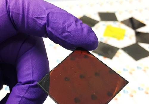
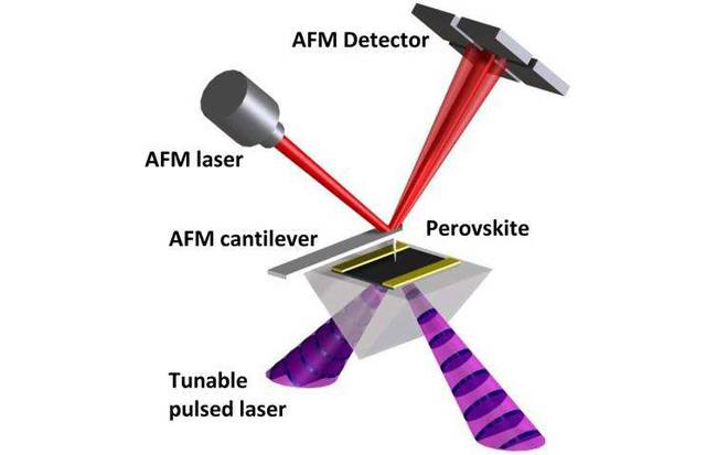
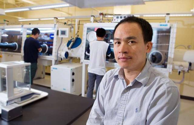
Jinsong Huang from the University of Nebraska collaborated with this research which will increase the durability of perovskite devices utilizing a property called ‘ferroelasticity’.

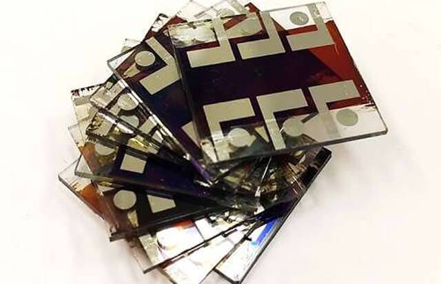
Our partners at Yale are also working on perovskite, here using an organic solvent to add stability and efficiency to the solar devices.

Our next visit is to Princeton, where Barry Rand’s team is turning perovskite around to emit light instead of harvesting it. Perovskite LEDs (or KiteLEDs as we really think they should be called) have arrived!

Biwu Ma from Florida State University has shed two out three dimensions to create a 1 dimensional perovskite matrix, allowing him to build a properly functional material one block at a time.

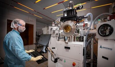
Having arrived in Brazil, our partner’s logistics team takes the lead, taking it out of the wooden box so that it can fit through the door of the facility. The journey resulted in the standard small bumps and dents that are categorized and logged so that our installation team can quickly and effectively get the system up and running, which they do.

Finally, all that’s left to do is to fabricate some superconducting circuits, and further the field of quantum computing. Our partners at Centro Brasileiro de Pesquisas Fisicas (CBPF) expressed their excitement at having gained the capabilities  of partnering with us in this translated LinkedIn post:


It is with great enthusiasm that we announce the arrival of the newest equipment, from Angstrom Engineering, to the Quantum Technologies Laboratory of CBPF. This laboratory is complementary to Labnano, one of the strategic laboratories of SisNANO – the National System of Nanotechnology Laboratories of the Ministry of Science, Technology and Innovation (MCTI).

SisNANO is comprised of a set of laboratories focused on research, development and innovation (RD&I) in nanosciences and nanotechnologies, with the essential characteristic of being multi-user and open access to public and private institutions.

Acquired with funding from Finep and support from MCTI, the new equipment will allow CBPF to advance in the manufacture of superconducting quantum nanodevices, such as Josephson junctions and SQUIDS. These devices are essential for the development of future quantum chips, which promise to transform areas such as computing, secure communication and metrology.

The impact of this advance is also connected to related projects funded by FAPERJ, CNPq and Petrobras, consolidating a robust research ecosystem in Brazil.

This achievement reinforces the commitment of CBPF and MCTI to leading the frontier of scientific research, contributing to enabling the country to compete in a global scenario marked by disruptive and strategic advances.

We would like to thank the institutions involved and the professionals who made this achievement possible. We invite the scientific, technological and industrial community to closely monitor the transformative results that this new infrastructure will provide.